French philosopher Jean-Baptiste Alphonse Karr famously said, "The greater the change, the more the same." These words are of great significance in the rapidly changing semiconductor industry. Currently, the industry is undergoing a profound technological change, driven by a variety of applications that require complex custom chip designs.
Breakthrough technologies such as artificial intelligence (AI), autonomous vehicles, edge processing, and small chips are causing rapid growth in the semiconductor market. Pioneering technologies are paving the way for high-growth markets, maintaining the competitive edge of products and driving the demand for increasingly complex system-on-chip (SoC) to support booming applications.
Due to the complexity of the design and the fierce competition in the market, innovative chip development strategies have become the key to rapid market entry and increasing revenue. Leveraging these technological advances is a strategic imperative to secure market leadership.
Mature hybrid design pattern
Over the past two decades, Oems, Tier 1 suppliers, and system designers have all adopted the hybrid chip design model, operating primarily independently. These companies often use customer owned Tools (COT) for chip design and subsequently work with back-end service companies and wafer production management teams.
The COT model requires the recruitment of dedicated semiconductor engineers from various disciplines to develop SOCs - a difficult task due to the scarcity and high cost of engineers. To meet this demand, companies often outsource talent to help manage temporary workload spikes and meet specific skill needs. However, this solution may not build a permanent, skilled team.
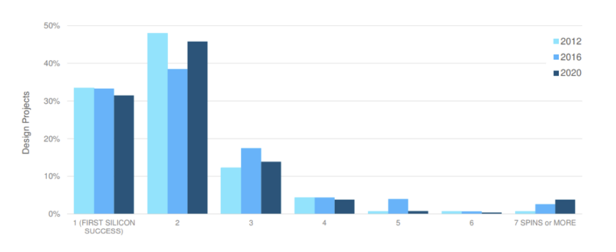
Large enterprises and startups alike must pay more attention to the serious financial impact of design errors, which can destroy budgets and delay getting to market. A leading EDA company revealed in a recent study that more than 60% of first-time designs require a silicon wafer redesign. With NRE costing millions of dollars each time, combined with the cost of delayed time-to-market, the increasing complexity of chip design greatly increases the risk of error, and any mistake can be career-ending

The 2020 Functional Validation study conducted by the Siemens EDA and Wilson research Group shows that only 32% of 2020 designs achieved first wafer success
Against this backdrop, the technology sector continues to experience growth in venture-backed startups, especially in the field of artificial intelligence. These agile companies typically adopt the COT model, but face similar obstacles when designing unique, complex chips for their products. The technical expertise required to create complex SOCs often goes beyond their core competencies.
This highlights the need for guidance from experienced partners throughout the chip design process. In addition, they are often unable to source wafers directly from industry-leading foundry TSMC, instead seeking value chain alliance (VCA) partners to make the mask and manage wafer production.
These trends have fueled a Renaissance of ASIC design firms, which now focus on "design and supply" services, offering clients a wide range of technology options. These companies have the technical skills to guide customers in making informed third-party IP choices and understand chip interconnect requirements, complex SoC power management, 3D packaging, and more.
In short, this minimizes the risk of new chip implementation and the corresponding financial impact. As a result, the new generation of ASIC companies have a wealth of experience and a stable engineering team that can provide reliable technical advice.
Model reform is imperative
Companies can prevent potential setbacks by partnering with a next-generation ASIC design and supply company that can manage the entire silicon wafer development process. This necessity has prompted a reassessment of chip design strategies. The pursuit of unique differentiation and shorter development cycles is driving companies to forge partnerships with their ASIC design partners.
This shift points to the need for a new model in which companies seek alternatives that can support the entire chip ecosystem, from idea to delivery. Adopting an integrated ASIC design and supply model offers significant advantages over traditional ASIC companies and reduces the investment associated with the COT model.
Integrating ASIC design and supply models involves cross-functional teams working closely with customers to define the entire semiconductor development and manufacturing process, including packaging, final testing, and product lifecycle management.
Today's SOCs are complex, multi-billion transistor devices that are customized for specific applications. The cost of developing such high-end chips can easily exceed $50 million, with photomask setup costs of $10 million to $20 million at advanced process nodes alone. Working with a technologically advanced single-source ASIC design company can speed up chip development and help ensure that silicon is a one-time success.
Highlighting the growing importance of ASIC-grade services, Rich Wawrzyniak, Principal Analyst at SHD Group, said, "In today's complex technology environment, ASIC-grade services have become an essential part of handling the implementation of advanced semiconductor designs."
In the face of rapidly evolving technology and pressure to accelerate time-to-market, it seems increasingly advantageous to work with a single-source ASIC design and supply company. With its expertise in managing the entire chip development process, such a company can help chip designers plan their future and secure a competitive advantage.


