On May 15, the Semiconductor Industry Association and the Boston Consulting Group released a 38-page report on the global chip industry, "The Resilience of the semiconductor supply chain is emerging."

According to the report, the semiconductor industry has become vulnerable to geographic concentration, with at least 50 points in the entire supply chain where one region holds more than 65% of the global market share.

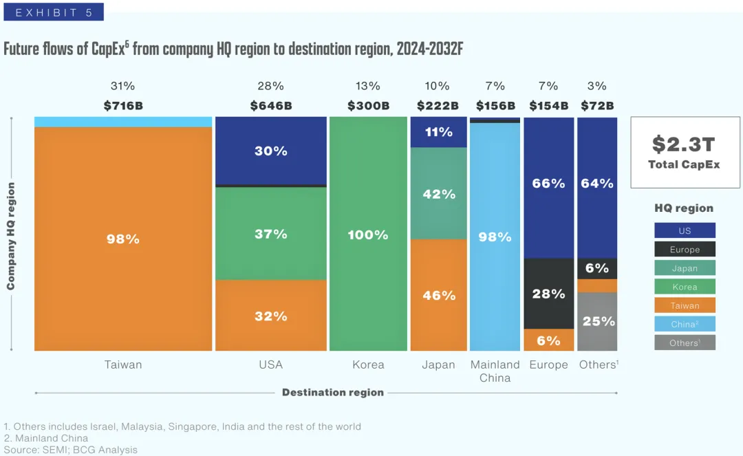
The report expects private sector investment in wafer manufacturing to be about $2.3 trillion in 2024-2032, compared to $720 billion in the 10 years prior to the enactment of the US Chip Act (2013-2022). The United States is expected to account for 28 percent of these capex, compared with a pace of just 9 percent of global capex prior to the Chip Act.
Without the Chip Act, the U.S. share is expected to fall to 8 percent of global capacity by 2032.
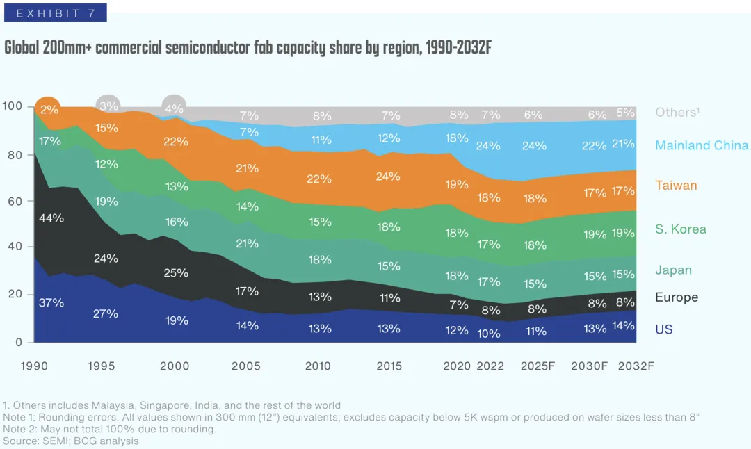
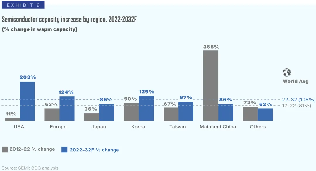
The report also predicts that by 2032, top wafer manufacturing capacity will expand from Taiwan and South Korea to the United States, Europe and Japan; Between 2022 and 2032, fab capacity in the United States will increase by 203 percent, the largest increase in the world. By 2032, the United States will reverse a decades-long decline and increase its share of global fab capacity to 14 percent from the current 10 percent.

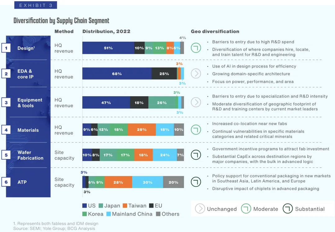
This report provides an updated view of the impact of current policies on future investment in the global semiconductor supply chain and its impact on resilience, broadly defined as an improvement in the geographic diversification of supply chains, and analyzes the likely impact of related industry trends over the next decade, forecasting changes in wafer manufacturing distribution and ATP capacity. The geographic diversification of other parts of the supply chain is also considered, including chip design, core IP, EDA, equipment, and materials.
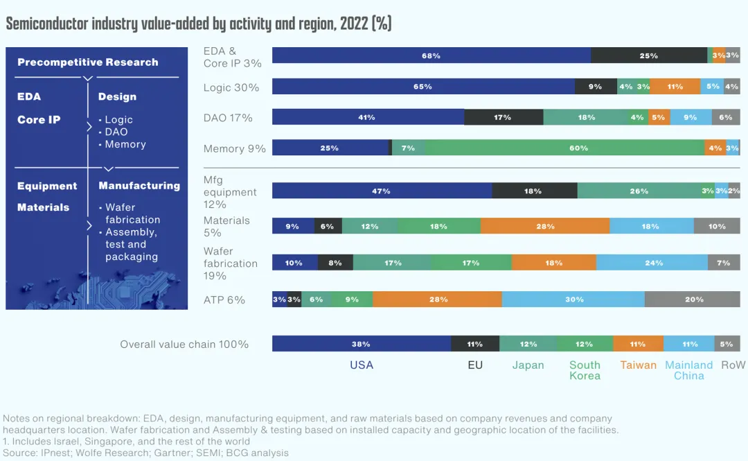
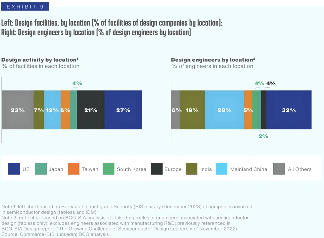
The global semiconductor supply chain is highly specialized, with different regions having advantages in different areas.

For example, companies headquartered in the United States are leading in chip design, core IP, and EDA; American, European and Japanese companies are leading in the field of equipment; China, Japan, Taiwan and South Korea lead in semiconductor materials; South Korean and Taiwan companies are leading in advanced chip manufacturing.
The globally integrated nature of the supply chain makes regional specialization possible, giving every specialized company access to the global market. However, geographic concentration also creates vulnerabilities, and significant geographic diversification is expected in the future, primarily in two areas, wafer manufacturing and encapsulation. Given the cost pressures, it is unlikely that a packaged-test assembly company will be headquartered in the United States, unless it is in some advanced packaging facility near a new fab.
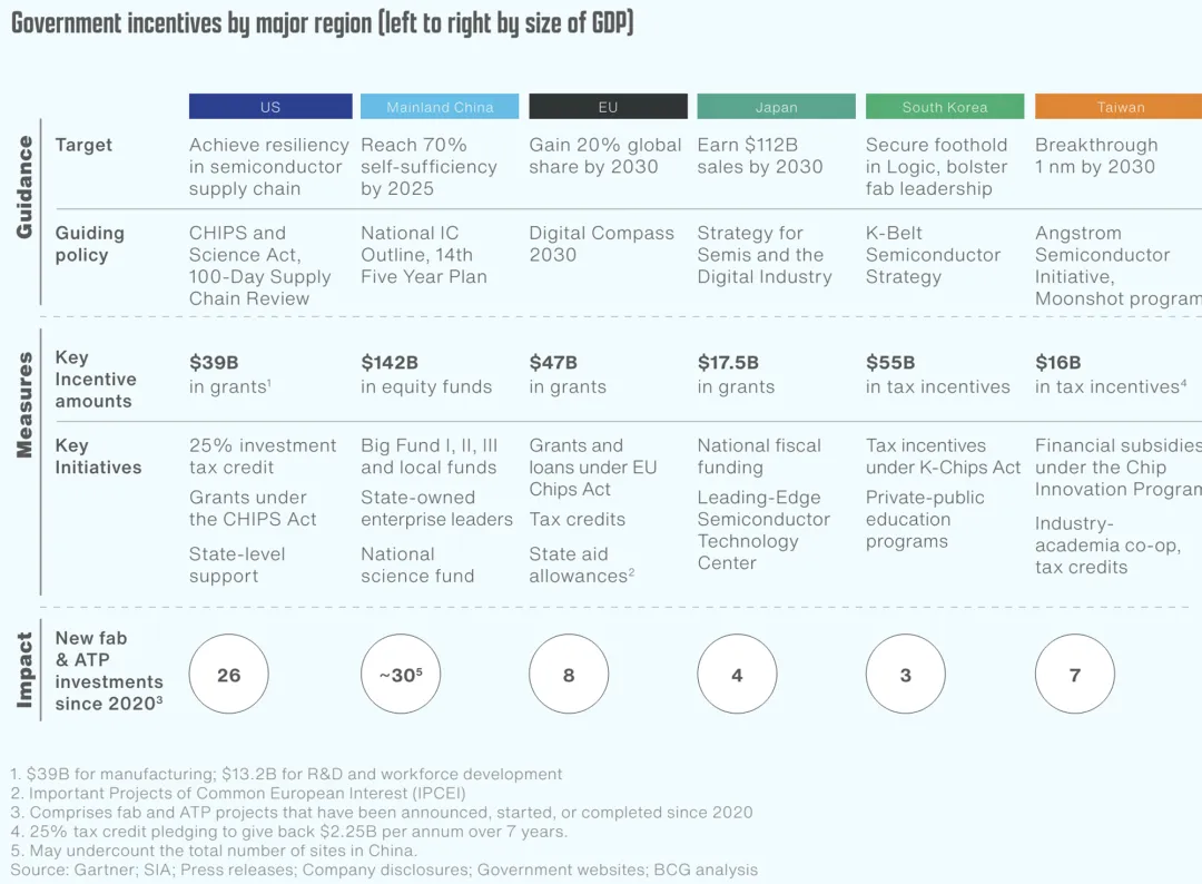
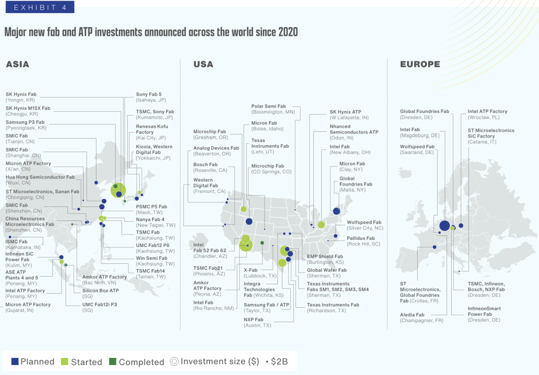
Taiwanese companies have announced plans to build seven new fabs on the island. Taiwan's chipmaking leader TSMC is also working with SONY, Denso and Toyota to boost manufacturing capacity at its Kumamoto plant in Japan.
Japanese chip manufacturing startup Rapidus has established an advanced 2nm chip production line at its new plant in Hokkaido. South Korea has announced a $47.1 billion plan to build 16 new fabs in a large chip cluster in Gyeonggi Province.
Between 2020 and the end of 2023, 80 new semiconductor manufacturing projects have been announced in the United States alone, which is expected to create 50,000 direct new jobs.
Europe has invested heavily in new capacity, with seven major fab investments announced since 2020. Much of the capacity is being built in eastern Germany, including Intel's investment in Magdeburg and TSMC's joint investment in a new plant in Dresden with leading European semiconductor manufacturers.
In the south of France, GF has partnered with ST to build a $3.1 billion fab in Croix. Poland is also preparing to open a new Intel Advanced packaging plant.
The report expects significant investment flows between regions between now and 2032.

Investing heavily in cutting-edge technologies can enable a region to compete at the forefront of innovation, but is not fully reflected in monthly wafer starts; On the other hand, investing in mature processes that allow a region to achieve more value for money and jobs in the short term risks creating excess capacity in parts where demand may be fixed or weakened.
Advanced Logic's investment model has become more decentralized globally, with Taiwanese and Korean companies significantly increasing their investments in the United States, Europe and Japan.
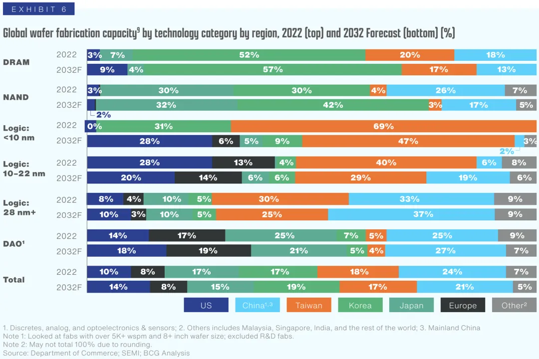
Advanced logic production will be distributed from almost 100% in South Korea and Taiwan by 2022 to more than 40% outside these regions by 2032.
In 2022, the United States did not produce any advanced logic chips. By 2032, the United States will produce nearly 30 percent of logic chips with processes smaller than 10nm.
When the planned fabs are operational, Europe and Japan will also produce about 12 percent of chips above 10nm.
Logic greater than or equal to 28nm will maintain a good distribution, with small share changes in most regions.

Among other process technologies, dynamic random access memory (DRAM) will remain highly concentrated in South Korea, but the U.S. share will increase three-fold from 3 percent to 9 percent.
The geographic concentration of NAND memory will increase. By 2032, South Korea's market share is expected to rise from 30 percent to 42 percent, with Japan and South Korea together accounting for about 75 percent of capacity.
Discrete, analog and optoelectronic chips (DAOs) will remain well distributed, with participation shares of 5% or higher across all major regions.
The net result of these specific, strategic and targeted initiatives by the company is to improve the resilience of the industry in terms of a more "average" share of global capacity by region. The United States will increase its share of global production capacity from 10% to 14%.

The report expects capacity to grow by more than 80% in every major region over the next decade. At 203 percent, capacity growth in the United States will be faster than in other regions and much faster than in the previous decade. In terms of thousands of wafers per month (300 mm equivalent), this means an increase from 1,121 KWH in 2022 (thousands of wafers per month) to 3,393 KWH in 2032 (a 203 percent increase).

At present, the Chinese mainland has more than 3,000 fab design companies, with annual revenues growing at double-digit rates. The Chinese Mainland's local chip design focuses on consumer electronics, industrial control systems and smart device chips, but in the advanced CPU, GPU and FPGA and the corresponding high-end server and computer power management is less competitive.

U.S. leadership in EDA should not be taken for granted.
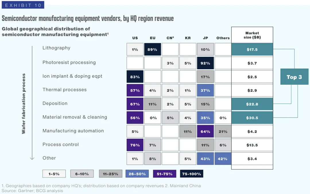
The $110 billion semiconductor equipment market covers more than 50 specialized devices, but concentration is high in some areas. The three segments of lithography, deposition, Material removal and cleaning account for 70% of the market share, each of which is dominated by a few major suppliers.

One European company holds 87% of the lithography market. In terms of deposition, material removal and cleaning, three companies (two in the United States and one in Japan) account for 70-80% of the market.
The top 15 equipment suppliers have production facilities in a total of 17 countries. The measures also include the establishment of new training centers to increase the pool of talent outside their regions.
Export controls in the United States, Japan and the Netherlands have increased the urgency of developing domestic alternatives. At least five Chinese producers are reportedly in mass production; Small and medium-sized enterprises have created lithography demonstration equipment; Naura and SMIC have entered the etching market for larger nodes.
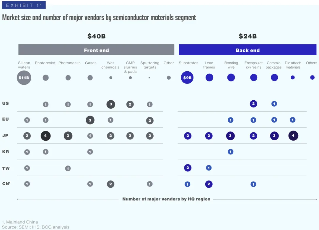
The $64 billion semiconductor materials market includes chemicals and materials used in the front end of the supply chain ($40 billion) and the back end ($24 billion ATP).

Silicon wafers and optical resist account for about half of the total front-end materials market ($19.5 billion), but other subcategories, such as gases, wet chemicals, CMP pastes, and sputtering targets, are also critical
to various steps in the manufacturing process. Similarly, substrate and lead frames account for about half of the back-end market ($12.8 billion).
Most of the leading semiconductor materials companies are headquartered in Japan, the United States and the European Union. There are at least three leading suppliers in Japan in multiple segments of the front-end
and back-end materials market.
A survey released in December 2023 by the U.S. Department of Commerce's Bureau of Industry and Security found that industry respondents "expressed serious concerns about domestic sources of three materials:
bare wafers, gases, and wet chemicals."
The post-pandemic chip shortage also highlights procurement challenges related to the packaging substrates that connect chips to circuit boards. In addition, certain raw materials, including gallium, rare earths and
many other key minerals, still originate primarily from a single region.
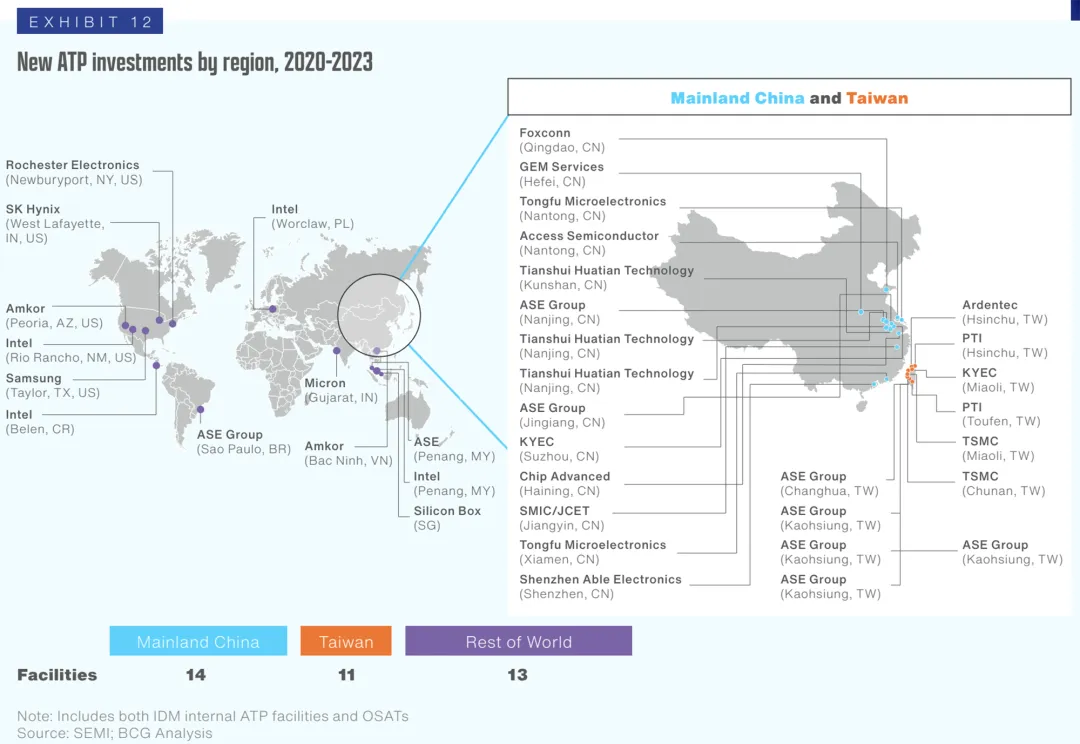
Currently, the $95 billion ATP market is mainly concentrated in Northeast Asia. South Korea has significant back-end capacity similar to existing fabs. China and Taiwan together have nearly 60% of the world's ATP
production capacity.

In the longer term, with continued policy support and overseas investment, the report expects ATP capacity to shift to other regions, including less developed regions in Latin America, Europe, and Southeast Asia. Southeast Asia is already the hub of ATP activity, accounting for around 20% of the global total.
In advanced packaging, which accounts for less than half of the ATP market, technological breakthroughs could open the door for high-cost regions such as the United States to play a bigger role in the ATP space. A key innovation is the heterogeneous integration of chiplets.
The first commercial results of the Chip Act's development of an advanced packaging ecosystem in the United States are being seen: Amkor announced it would build a $2 billion plant in Peoria, Arizona, to package chips manufactured by TSMC for Apple; Intel will invest $3.5 billion in advanced packaging at its facility in Rio Rancho, New Mexico; SK Hynix plans to invest about $4 billion to build an advanced packaging plant in Indiana, USA; Samsung also plans to build an advanced packaging plant in Texas.
One potential area of concern is the ≥28nm logic. If the trajectory does not change, the high utilization driven fabs economy could lead to significant pressure to lower wafer prices, which could cause fabless companies to reconsider process technology choice decisions.

Over the next decade, semiconductors will play a key role in the global economy, from everyday products to the forefront of defense and artificial intelligence.
There are few industries where supply chains and ecosystems are so complex and intertwined on a global scale. However, a number of factors, from geopolitical tensions and a more complex regulatory environment to labor shortages and rising costs, underscore the need to diversify and invest in supply chains to improve resilience.
Similarly, governments recognize the strategic importance of semiconductors and seek to reduce strategic dependence by attracting and incentivizing new local or nearby investments. But resilience is not the same as self-sufficiency, and the costs of self-sufficiency would be staggering.


